- Çalışma Saatleri : 08:30 - 18:00

Yüksek Adetli Sipariş Zorunluluğu YOK!
Bizden ihtiyacınız olan PCB miktarı kadar baskı devre kartı sipariş edebilirsiniz. Prototip PCB çalışmalarınız için mikro CNC’ler ile kazıma yöntemiyle üretimini gerçekleştirdiğimiz tek çift katman pcb’lerden maskesiz yani renksiz ve malzeme baskısız olarak minimum 1 adet, orta ölçekli, az adetli ihtiyaçlarınız için renkli, kalay kaplamalı standart üretim baskı devre kartları için minimum 5 adet olarak tasarımlarınız için sipariş verebilirsiniz. İhtiyacınız olmayan adet kotalarını satın almaya müşterilerimizi zorlamayız.

Tooling Ücreti YOK!
Elektronik mühendisleri, öğrenciler ve amatör olarak elektronik gelistirme ile ugraşan hobiciler için prototip PCB, düşük hacimli PCB imalat ve PCB montaj ihtiyaçları için uygun fiyat ve kaliteli üretim seçenekleri ile elimizden gelenin en iyisini yapıyoruz.

PCB Prototipleme
Prototipleme aşaması, mühendisler, öğrenciler ve hobi olarak elektronik ile ugraşanlar için en heyecan verici ve sabırsız zaman aralığıdır. AR-GE çalışmalarınız için prototip PCB çalışmalarınızı 24 saat içinde üreterek teslim ediyoruz!

Küçük Hacimli Üretim
Müşterilerimiz için PCB prototipleme üretim hizmetimizden ayrı olarak, düşük hacimli üretim ve 30 adetten 10.000 adete kadar az miktarda, orta hacimli ve yüksek adette tek yüzlü ve delik içi kaplamalı çift yüzlü baskı devre kartları hizmetleri sunmaktayız.


Bir PCB Üretiminin Adımları Nelerdir?
Standart baskılı devre kartı diye bir şey yoktur. Her elektronik projenin ve PCB’nin belirli her bir fonksiyonu farklı bir ürün için benzersiz bir elektriksel işlevi vardır. Bu nedenle, bir PCB baskı devre kartnı üretmek, birçok adım ve prosesten olusmaktadır.
CAD/CAM İŞLEM MERKEZİ ÜRETİM ÖNCESİ İNCELEME
PCB SABLON VE KURU FİLM ÇIKTISI HAZIRLIK
POZLAMA ve GÖRÜNTÜ ALMA
PCB YÜZEY ASINDIRMA
DELİK AÇMA
DELİK İÇİ KAPLAMA
SOLDERMASK *YÜZEY KORUYUCU BOYA
YÜZEY KAPLAMA *HAL KAPLAMA
V-CUT KESİM
ELEKTRİKSEL TEST VE SON KONTROL
1. PCB - Rijit Elektronik Baskı Devre Kartı Üretim Kapasitesi
| Features | Capability | Notes |
| Layer count | 1-20 Layers | The number of copper layers in the board. |
| Controlled Impedance | 4/6 layer, default layer stack-up | Controlled Impedance PCB Layer StackupJLCPCB Impedance Calculator |
| Material | FR-4 Aluminum Copper core Rogers / PTFE Teflon | FR-4: Tg 135 / Tg140 / Tg155 / Tg170 Aluminum thermal conductivity: 1W/m.K Copper core thermal conductivity: 380W/m.K |
| Dielectric constant | 4.5(double-sided PCB) | 7628 Prepreg 4.4 3313 Perpreg 4.1 2216 Perpreg 4.16 |
| Max. Dimension | 400x500mm | The maximum dimension JLCPCB can accept |
| Dimension Tolerance | ±0.1mm | ±0.1mm(Precision) and ±0.2mm(Regular) for CNC routing, and ±0.4mm for V-scoring |
| Board Thickness | 0.4 – 2.5 mm | Thickness for FR4 are: 0.4/0.6/0.8/1.0/1.2/1.6/2.0 mm (2.5 mm only available with 12 layers or more. ) |
| Thickness Tolerance ( Thickness≥1.0mm) | ± 10% | e.g. For the 1.6mm board thickness, the finished board thickness ranges from 1.44mm(T-1.6×10%) to 1.76mm(T+1.6×10%) |
| Thickness Tolerance ( Thickness<1.0mm) | ± 0.1mm | e.g. For the 0.8mm board thickness, the finished board thickness ranges from 0.7mm(T-0.1) to 0.9mm(T+0.1). |
| Finished Outer Layer Copper | 1 oz / 2 oz (35um / 70um) | Finished copper weight of outer layer is 1oz or 2oz. |
| Finished Inner Layer Copper | 0.5 oz / 1 oz / 2 oz (17.5um / 35um / 70um) | Finished copper weight of inner layer is 0.5oz by default. |
| Surface Finish | HASL (leaded / lead-free), ENIG, OSP (copper core boards only) | FR4 has all three finishes available, 6+ layers and RF boards only have ENIG. Aluminium core boards only have HASL. Copper core boards only have OSP. |
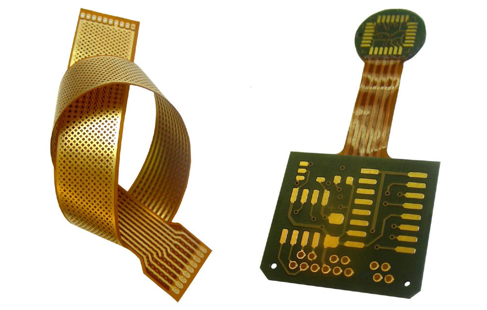
2. FPCB - Esnek Elektronik Baskı Devre Kartı Üretim Kapasitesi
| Category | Features | Capability | Description |
| Layer Count | 1 layer,2 layers | The number of copper layers in the FPC | Rigid-flex PCBs are not yet supported. |
FPC Stack-Up | Single-Sided | FPC with copper and coverlay on the same one side only. Inner PI thickness: 25 μm | |
| Double-Sided | FPC with copper on both sides. Inner PI thickness: 25 μm | ||
Dimensions | Maximum Dimensions | Regular: 234 × 490 mm | Absolute limit of 250 × 500 mm allowed with mandatory handling edges – confirm with customer support before ordering |
| Minimum Dimensions | No limit, but FPCs whose dimension is smaller than 20 × 20 mm are best panelised | See Flex PCB panel design guidelines | |
| FPC Finished Thickness | Single-sided: 0.07 / 0.11 mm Double-sided: 0.11 / 0.12 / 0.2 mm | The thickness of the finished FPC excluding any stiffeners(If the measured area has no copper or coverlay, the finished thickness will be reduced.) | |
| Outer Layer Copper Weight | Single-sided: 18 μm (0.5 oz), 35 μm (1 oz) Double-sided: 12 μm (0.33 oz), 18 μm (0.5 oz), 35 μm (1 oz) | The thickness of copper on the FPC | |
| Type of Process | Dry film process with LDI (laser direct image) exposure technology | LDI provides higher accuracy than traditional LED exposure. The machines also support automatic alignment based on board size to eliminate pad offset issues. | |
| Surface Finish | ENIG. Thickness: 1u\” / 2u\” | ENIG deposits a nickel-gold coating on exposed pads to prevent oxidation. | |
| Thickness with Stiffener | Thickness with Stiffener = FPC Thickness + Stiffener Thickness | See the PI Stiffener Thickness Calculator | |
| FPC Thickness Tolerance | ±0.05 mm | Additional tolerance exists for stiffeners. Thicker stiffeners have larger tolerances. | |
Holes | Hole Diameter | 0.15-6.5 mm | The recommended maximum diameter for PTHs is 5 mm, if bigger may cause risks to production |
| Diameter Tolerance | ±0.08 mm | Example: A 1.00 mm designed diameter is allowed to yield any physical diameter between 0.92-1.08 mm. | |
| Minimum Plated Slot | 0.50 mm | ||
| Minimum Non-Plated Slot | Not limited | At least 0.2 mm copper clearance is required around non-plated slots. | |
| Castellated Holes | Castellated holes are plated half-holes on the edge of an FPC. Most often used for press-soldered connectors. ① Castellated hole diameter: ≥ 0.3 mm ② Castellated hole to board edge: ≥ 0.5 mm ③ Castellated hole to hole: ≥ 0.4 mm | ||
| Min. Via hole size/diameter | 0.15 mm (Via hole size)/ 0.35 mm (Via diameter) ① Annular ring: 0.1 mm minimum, 0.125 mm recommended ② Recommended via size: 0.3 mm inner, 0.55 mm outer | ||
Traces | Annular Ring for PTH | ≥ 0.25 mm recommended, absolute limit: 0.18 mm | |
| Minimum Trace Width/Spacing (1 oz) | ① 12 μm (0.33 oz) copper: 3/3 mil (absolute limit 2/2 mil – avoid if possible) ② 18 μm (0.5 oz) copper: 3.5/3.5 mil ③ 35 μm (1 oz) copper: 4/4 mil These are regular capabilities. Contact customer support for custom capability requirements. | ||
| Trace Width Tolerance | ±20% | Example: A 0.10 mm designed trace width is allowed to yield any physical width between 0.08-0.12 mm. | |
| Pad-to-Trace Clearance | ① Via ring to trace: ≥ 0.1 mm (more whenever possible) ② Exposed pad to trace:≥ 0.15 mm (more whenever possible) | ||
| NPTH to Copper Clearance | ≥ 0.20 mm | The clearance from an NPTH to traces, pads, and copper pours | |
| BGA | ① BGA pad diameter: ≥ 0.25 mm ② BGA pad to trace clearance: ≥ 0.2 mm | ||
Coverlay/ Soldermask | Coverlay Color | Yellow / Black / White | Yellow is recommended |
| Coverlay Opening | Coverlay expansion (one-sided): 0.1 mm Coverlay opening to trace clearance: ≥ 0.15 mm (more whenever possible) | ||
| Via covering | Recommended to keep coverlay over vias | ||
| Coverlay Thickness | ① PI: 12.5 μm, glue: 15 μm (on 12/18 μm copper) ② PI: 25 μm, glue: 25 μm (on 35 μm copper) | ||
| Minimum solder bridge width | 0.5 mm minimum, i.e. solder bridge narrower than 0.5 mm will be removed. Contact customer support for any non-standard requirements. | ||
Silkscreen | Character Height | ≥ 1mm (More in case of complex patterns or knock-out text) | |
| Character Line Width | ≥ 0.15mm (Narrower lines do not print well) | ||
| Character to Pad Clearance | ≥ 0.15mm (Any silkscreen closer to a pad than this will be clipped) | ||
FPC Outline | Laser Outline | ① Copper to board edge ≥ 0.3mm ② Copper to slots ≥ 0.3mm ③ Outline tolerance: ±0.1 mm (±0.05 mm upon request) | |
| Gold Finger Pad to Board Edge Clearance | 0.2 mm. Gold fingers will be cut back if exceeding this clearance to avoid damage during laser cutting the outline. Castellated pads are exempt from this clearance. | ||
| Panels (See FPC Panel Design Guide) | ① Spacing between boards is commonly 2 mm. For boards with metal stiffeners use 3 mm instead. ② Handling edges of width 5 mm required on all four sides. Copper pour is required on these edges, with 1 mm clearance around fiducials and 0.5 mm clearance around tooling holes. ③ Fiducials: 1 mm; tooling holes: 2 mm; Fiducial centre to board edge: 3.85 mm. Add four fiducials with one offset by 5 mm or more to aid orientation. ④ Support tab width: 0.7-1.0 mm ⑤ Maximum panel size: 234 × 490 mm | ||
Stiffeners (Detailed Introduction) | PI Stiffener | Thickness options: 0.1 mm, 0.15 mm, 0.20 mm, 0.225 mm, 0.25 mm | PI stiffeners are most often used with gold finger connectors. For example if the connector needs to be 0.3 mm thick on a 0.11 mm FPC, a 0.225 mm stiffener thickness is most suitable. |
| FR4 Stiffener | Thickness options: 0.1 mm, 0.2 mm | FR4 is usually only used on low-end products because it is prone to chipping. Avoid if possible. | |
| Stainless Steel Stiffener | Thickness options: 0.1 mm, 0.2 mm, 0.3 mm | Steel stiffeners cost more but have excellent flatness and do not easily deform. This makes them good as support under SMD components. Note that since steel is slightly magnetic it should not be used with hall effect sensors or similar components. | |
| 3M Tape | 3M9077 (0.05 mm thick; heat-resistant) 3M468 (0.13 mm thick; not heat-resistant) | Usually used to secure FPCs after assembly | |
| EM Shielding Film | 18 μm thick, black. Helps lower EMC. The recommended practice is to add soldermask openings over edge guard rails to electrically connect them to the shield films. | ||
Design Considerations | Impedance Calculation | Core polyimide εr: 3.3 Coverlay εr: 2.9 Core polyimide thickness: 25 μm | Impedance measurement and control are not yet supported. Traces are only controlled for width and the customer is responsible for choosing trace widths to achieve their impedance requirements. |
| EasyEDA (Highly Recommended) | EasyEDA supports a dedicated stiffener layer. The shape and thickness of stiffeners are set and embedded in the design document so they don’t need to be entered manually when ordering. See how to design FPC at EasyEDA | ||
| Other EDA Software | Put annotations on its own layer. Include the outlines of the stiffeners and indicate material and thickness. This information is not automatically parsed so stiffener options need to be set manually when ordering. Make sure that annotation text does not overlap the board area. | ||
| Other Design Constraints | Same requirements as rigid PCBs in terms of holes, traces, soldermask, and silkscreen. |